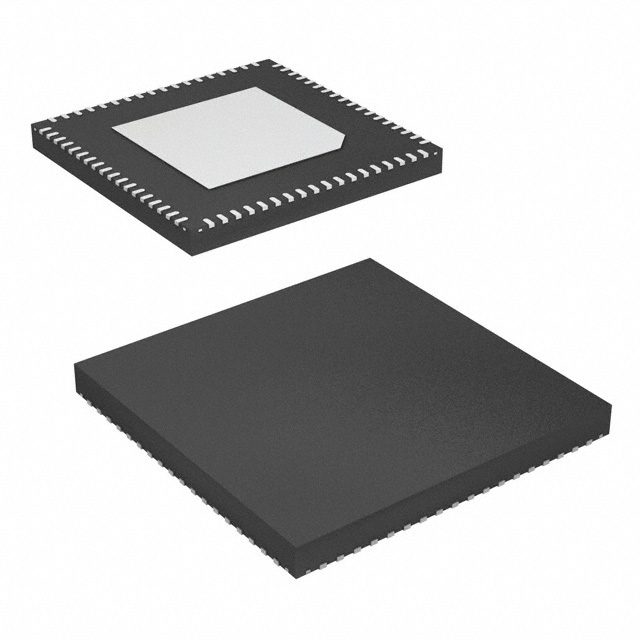
The Renesas 8T49N203A-029NLGI is a versatile timing device designed primarily for high-performance clock generation and distribution applications. It is part of the 8T49 family of integrated circuits, which are known for their reliability and precision in timing applications.
Functions
- Clock Generation: Produces multiple clock frequencies from a single reference clock.
- Jitter Reduction: Utilizes advanced techniques to minimize timing jitter.
- Programmable Output: Configurable output frequencies via internal registers, allowing for flexibility in applications.
- Output Modes: Supports various output formats such as LVDS, LVCMOS, and more, making it adaptable to various systems.
- Phase Adjustments: Allows for fine adjustments in phase, which is crucial for synchronization in complex systems.
Applications
- Telecommunications: Used in synchronous optical networks (SONET), packet networks, and other telecom applications that require precise timing.
- Data Centers: Important for clocking in high-speed networks and servers.
- Consumer Electronics: Found in devices requiring multiple synchronized clock signals.
- Automotive Systems: May be used in advanced driver-assistance systems (ADAS) for precise timing.
- Industrial Automation: Essential for timing in control systems and machinery.
Alternative Components
- Si5351/Si5352 (Skyworks): A versatile clock generator that is programmable and has a range of output frequencies.
- CDCM61005 (Texas Instruments): A clock generator known for low jitter and multiple output configurations.
- LMK04832 (Texas Instruments): A high-performance clock synthesizer that supports a wide range of applications.
Embedded Modules
As an integrated circuit, the 8T49N203A-029NLGI does not typically come in “modules” but can be integrated into various custom PCB designs. However, it may be available in development kits or evaluation boards that include the chip along with supporting components to facilitate testing and integration.
Related Q&A
Q1: What types of output signals does the Renesas 8T49N203A support?
- A1: The device supports various output signal types, including LVDS (Low Voltage Differential Signaling), LVCMOS (Low Voltage Complementary Metal-Oxide-Semiconductor), and other formats for compatibility with different system designs.
Q2: How can the output frequency of the 8T49N203A be programmed?
- A2: The output frequencies can be programmed via an I2C/SPI interface, allowing users to write to internal registers that control the frequency and configuration settings of the outputs.
Q3: What considerations should be made when designing with the 8T49N203A in a PCB?
- A3: Key considerations include the layout for differential pair signals, power supply decoupling, grounding techniques to reduce noise, and ensuring proper trace lengths to minimize signal integrity issues.
Q4: Can the 8T49N203A be used in applications requiring high phase accuracy?
- A4: Yes, this device allows for phase adjustments and is designed to meet the requirements of applications that need precise timing and synchronization among multiple outputs.
Q5: What is the maximum power consumption of the 8T49N203A?
- A5: The maximum power consumption is typically specified in the datasheet, but it is generally optimized for low power operation, making it suitable for battery-operated and energy-efficient designs.
This overview should provide you with a solid understanding of the Renesas 8T49N203A-029NLGI device and its applications in the realm of integrated circuits.


 8T49N203A-029NLGI Datasheet