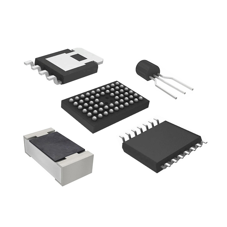
Images are for reference only.
First-time registration with orders over $2,000 receives a $100 coupon. Register Now !


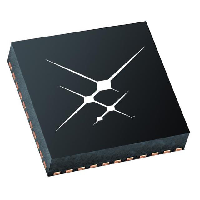
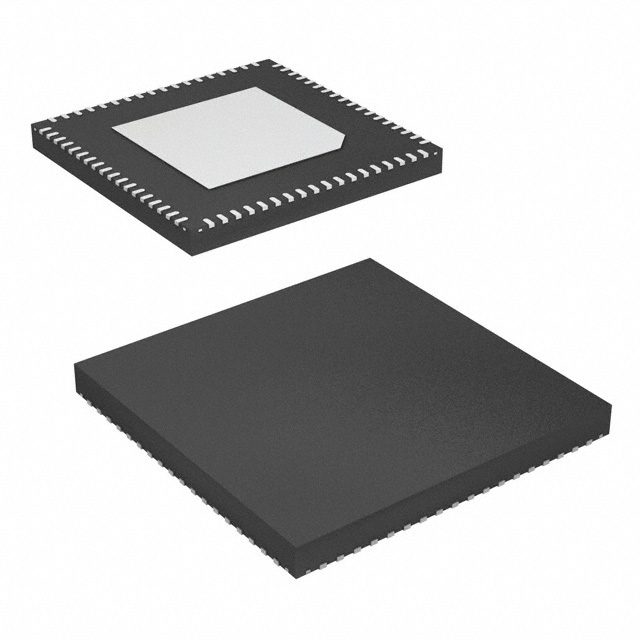
Renesas Electronics 8T49N203A-009NLGI8
IC TRANSLATOR UNIV FREQ 40VFQFN
 8T49N203A-009NLGI8 Datasheet
| Quantity | Unit Price | Total |
Help you to save your cost and time
Strict quality inspection and Reliable package for goods
Fast Reliable delivery to save time
Provide 365 days warranty after-sales service
8T49N203A-009NLGI8 information
Renesas Electronics 8T49N203A-009NLGI8 technical specifications, attributes, parameters.
- Category:Integrated Circuits (ICs)/Clock Generators, PLLs, Frequency Synthesizers
- Product Status:Obsolete
- Operating Temperature:-40°C ~ 85°C
- Mounting Type:Surface Mount
- Package / Case:40-VFQFN Exposed Pad
- Supplier Device Package:40-QFN (6x6)
- Frequency - Max:156.25MHz
- Number of Circuits:1
- Output:LVDS
- Voltage - Supply:2.375V ~ 3.465V
- P L L:Yes with Bypass
- Input:HCSL, LVDS, LVHSTL, LVPECL, Crystal
- Ratio - Input: Output:3:2
- Differential - Input: Output:Yes/Yes
- Divider/ Multiplier:Yes/No
- Series:FemtoClock® NG
- Packaging:Tape & Reel (TR)
Related Products Recommended


You can place an order after registration or purchase products directly as a visitor.
2.Search product
Search to find the part number of the product you need to order.
3.Add to cart
After finding the product. Then add the products to your shopping cart directly.
4.Filling Address and Secure Checkout
Please fill the shipping address and express information when placing your order.
5.Pay the orders
You can pay the orders on the website directly or pay by wire transfer offline. We support: Paypal ,VISA , WIRE TRANSFER.
6.Tracking Your Order
We will dispatch your order within 24 hours and provide you with a tracking number. You can also check the order information on the website or contact our sales staff for tracking.
7.Sign for order and evaluate
Sign for your order,and provide your shopping review here!
We can prompt fulfill customer requests for electronic components, even for scarce parts in the market.