Xilinx Zynq-7000 Series SoC: XC7Z010-1CLG400C
XC7Z010-1CLG400C is a Zynq-7000 series SoC (system-on-chip) launched by Xilinx, which combines ARM processor and FPGA architecture and is suitable for embedded system design.
XC7Z010-1CLG400C Technical Specifications
▶Core Architecture
Integrated architecture: Based on Xilinx SoC architecture, the dual-core ARM Cortex-A9-based processing system (PS) and 28nm Xilinx programmable logic (PL) are integrated into the same chip.
Internal connection: High-bandwidth connection based on ARM AMBA® AXI is used inside the PS and between the PS and PL, and QoS support is provided on key hosts for latency and bandwidth control.
▶Memory resources
Cache: 32KB 1-level 4-way set-associative instruction and data cache (independent of each CPU), that is, L1 cache instruction memory and L1 cache data memory are both 2×32kB; 512KB 8-way set-associative L2 cache (shared between CPUs).
On-chip RAM: 256KB on-chip RAM (OCM), and on-chip boot ROM.
External storage support: Byte parity support external memory interface, multi-protocol dynamic memory controller, support 16-bit or 32-bit interface of DDR3, DDR3L, DDR2 or LPDDR2, ECC support in 16-bit mode, 1GB address space, support static memory interface, parallel NOR flash, ONFI1.0 NAND flash (1-bit ECC), 1-bit SPI, 2-bit SPI, 4-bit SPI (quad SPI) or two quad SPI (8-bit), etc.
▶Interfaces and peripherals
DMA controller: 8-channel DMA controller, supporting memory-to-memory, memory-to-peripheral, peripheral-to-memory scatter-gather transactions.
Ethernet: Two 10/100/1000 triple-speed Ethernet MAC peripherals with IEEE Standard 802.3 and IEEE Standard 1588 Revision 2.0 support, scatter-gather DMA capability, GMII, RGMII, and SGMII interfaces.
USB: Two USB 2.0 OTG peripherals, each supporting up to 12 endpoints, USB 2.0-compatible device IP core supporting mobile, high-speed, full-speed, and low-speed, Intel EHCI-compatible USB host, with 8-bit ULPI external PHY interface.
Others: two CAN bus interfaces, two SD/SDIO 2.0/MMC3.31 compatible controllers, two full-duplex SPI ports, two high-speed UARTs (up to 1Mb/s), two master I2C and slave I2C interfaces, with four 32-bit groups of GPIO, up to 54 flexible multiplexed input/output (MIO).
▶Packaging and physical characteristics
Packaging form: 400-LFBGA, CSPBGA packaging, supplier device packaging is 400-CSPBGA (17x17).
Number of I/Os: 130
Operating temperature: 0℃~85℃.
▶Application fields
Automotive field: It can be used for body control, in-vehicle infotainment system, etc. in automotive electronic systems.
Industrial control: It can realize functions such as industrial automation control and monitoring system.
Communication field: It is suitable for scenarios with high requirements for data processing and logic control such as network equipment and communication base stations.
XC7Z010-1CLG400C Similar or Alternative Comparison
XC7Z010-1CLG400C vs XC7A15T-1CSG325I vs XC7A15T-1CSG325C vs M2GL005-VF400 vs M2GL005-VFG400
| parameter | XC7Z010-1CLG400C | XC7A15T-1CSG325I | XC7A15T-1CSG325C | M2GL005-VF400 | M2GL005-VFG400 |
|---|---|---|---|---|---|
| Image | 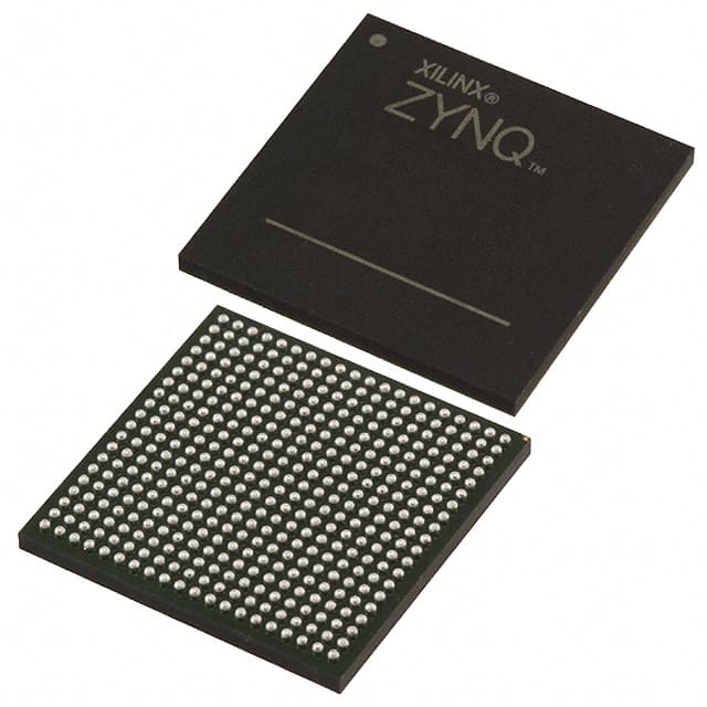 |  |  |  |  |
| Manufacturer | Xilinx | Xilinx | Xilinx | Microchip | Microchip |
| Package / Case | 400-LFBGA、CSPBGA | 400-LFBGA | 400-LFBGA | 324-LFBGA, CSPBGA | 324-LFBGA, CSPBGA |
| Number of Pins | 400 | 400 | 400 | 325 | 325 |
| Number of I/O | 130 | 169 | 169 | 150 | 150 |
| RAM Size | 256KB | 87.9 kB | 87.9 kB | 112.5 kB | 112.5 kB |
| Supply Voltage | 1 V | 1.2 V | 1.2 V | 1 V | 1 V |
| Terminal Position | BOTTOM | BOTTOM | BOTTOM | BOTTOM | BOTTOM |
| Packaging | Tray | Tray | Tray | Tray | Tray |
| Terminal Pitch | 0.8 mm | 0.8 mm | 0.8 mm | 0.8 mm | 0.8 mm |
XC7Z010-1CLG400C Datasheet PDF
FAQs for XC7Z010 - 1CLG400C
What are the power supply requirements for XC7Z010 - 1CLG400C?
XC7Z010 - 1CLG400C requires multiple power supply voltages, such as 1.0V core power supply, 1.8V/3.3V I/O power supply, etc. Different power supply voltages power different parts of the chip to ensure their normal operation. When designing a power supply circuit, it is necessary to ensure that the stability and ripple of the power supply meet the requirements of the chip. Usually, a power management chip is required to provide a suitable power supply.
What are the pin distribution and functions of the chip?
XC7Z010 - 1CLG400C uses a 400-pin LFBGA package with rich pin functions, including power pins, clock pins, I/O pins, configuration pins, etc. The specific pin functions can be referred to the chip data sheet. When designing hardware, these pins need to be reasonably allocated and used according to design requirements.
How to deal with the heat dissipation problem of the chip?
Since XC7Z010 - 1CLG400C will generate a certain amount of heat when working, effective heat dissipation treatment is required. Heat dissipation devices such as heat sinks and fans can be used to dissipate the heat generated by the chip. When designing PCBs, the heat dissipation efficiency can also be improved by adding heat dissipation vias and reasonably laying out copper foil.
What development tools are needed to develop XC7Z010 - 1CLG400C?
Xilinx's Vivado Design Suite is mainly needed for hardware design, synthesis, implementation and bitstream file generation, as well as PetaLinux Tools for embedded Linux system development. If bare metal development is performed, Xilinx SDK is also required for software development and debugging.
How to run an embedded Linux system on XC7Z010 - 1CLG400C?
First, use PetaLinux Tools to create a PetaLinux project and configure system parameters, including kernel, file system, driver, etc. Then compile the system, generate a BOOT.bin file, download it to the development board, and you can start the embedded Linux system.
What application scenarios is XC7Z010 - 1CLG400C suitable for?
It is suitable for automotive electronics, industrial control, communication equipment and other fields. For example, in automotive electronics, it can be used for body control and in-vehicle infotainment systems; in industrial control, it can realize industrial automation control and monitoring systems; in communication equipment, it can be used for network equipment, communication base stations, etc.