How to determine the CL value of load capacitance?
Load capacitance is a key parameter in the design of crystal oscillator circuits. It has a direct impact on the frequency characteristics and stability of the crystal oscillator. The load capacitance is not the capacitance of a single component, but the total capacitance formed by the external capacitors at both ends of the crystal oscillator and the parasitic capacitance in the circuit.
Appropriate load capacitance is a key step to ensure the stable operation of the crystal oscillator. Inappropriate load capacitance may cause the following problems:
1. Frequency offset: If the load capacitance is too large or too small, the oscillation frequency of the crystal may deviate from its nominal value, resulting in inaccurate system clock.
2. Startup problems: Inappropriate load capacitance may make it difficult for the oscillator to start, especially when the power supply voltage is low or the temperature changes greatly.
3. Poor stability: Load capacitance mismatch may cause the frequency stability of the oscillator to deteriorate, affecting the reliability of the system.
4. Increased power consumption: Inappropriate load capacitance may cause increased power consumption of the circuit, affecting the battery life of battery-powered devices.
5. Signal integrity issues: Frequency instability may cause signal integrity issues, affecting the accuracy of data transmission and processing.
Load capacitance refers to the capacitance value required for the crystal oscillator to work stably at its nominal frequency. It is determined by both the external capacitor and the parasitic capacitance of the circuit board.
Crystal specification:
The load capacitance value can be found in the specification of the passive crystal. Taking the KOAN resonator KX32 as an example, the load capacitance is between 8 and 32pF.


Estimating parasitic capacitance:
Parasitic capacitance on the circuit board is inevitable, mainly from the capacitance of the PCB traces and pads. The general parasitic capacitance value is between 2 and 5pF. Estimating parasitic capacitance is a key step in selecting a suitable external capacitor. If the parasitic capacitance is low (such as 1-2pF), it may be more appropriate to select a smaller load capacitance (such as 12.5 pF). Lower parasitic capacitance means that more load capacitance needs to be compensated by external capacitance to achieve the total CL.
Here are the methods to estimate parasitic capacitance:
1. Most PCB design software has the function of extracting parasitic parameters, which can estimate the parasitic capacitance of pads and traces.
2. Use a capacitance meter to measure the capacitance value on the actual circuit board. Remove the crystal and measure the capacitance at both ends of the crystal mounting position.
3. Estimation based on the experience of similar circuit designs can usually be used as a preliminary reference.
Calculate external capacitance:
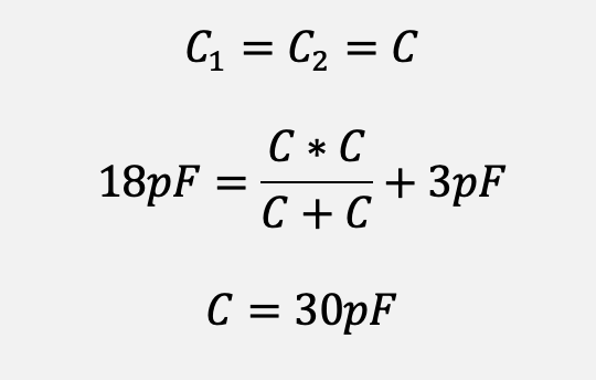
Calculate external capacitance C1 and C2 based on the load capacitance and parasitic capacitance of the crystal:

Assuming that the load capacitance of the crystal you choose is 18pF and the estimated parasitic capacitance is 3pF, two 30pF external capacitors are required.

Test:
Use a frequency meter or oscilloscope to check whether the oscillation frequency is within the expected range. If the test result is not ideal, it can be optimized by adjusting the external capacitance value. During the design stage, you can use adjustable capacitors for fine-tuning to find the best load capacitance value.
